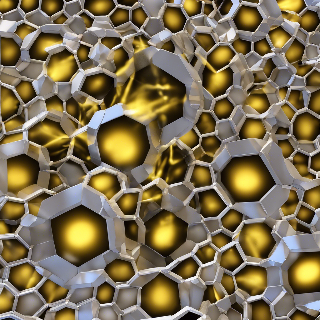
University of Manchester researchers develop a clean and precise technique for transferring 2D crystals, enabling the creation of atomically perfect stacks and advancing the commercialization of 2D material-based electronic devices.
Researchers at the University of Manchester have achieved a significant breakthrough in the transfer of 2D crystals, bringing us closer to the commercialization of next-generation electronics. In a recent article published in Nature Electronics, the team describes a new technique that utilizes an inorganic stamp to create the cleanest and most uniform 2D material stacks to date. Led by Professor Roman Gorbachev, the researchers successfully “pick and place” 2D crystals into van der Waals heterostructures, achieving atomically clean interfaces over extended areas. This breakthrough has the potential to revolutionize the field of 2D materials and open up new possibilities for electronic devices.
Precise Stacking and Clean Interfaces
The precise stacking of individual 2D materials in defined sequences offers the ability to engineer designer crystals at the atomic level, resulting in novel hybrid properties. While various techniques have been developed to transfer individual layers, most rely on organic polymer membranes or stamps for mechanical support during the transition from the original substrates to the target ones. Unfortunately, these organic materials introduce surface contamination to the 2D materials, even in controlled cleanroom environments. This contamination hinders the development of industrially viable electronic components based on 2D materials.
Overcoming Transfer-Induced Contamination
Surface contaminants trapped between 2D material layers often segregate into isolated bubbles, leaving atomically clean areas. However, the clean areas are typically confined to small regions, limiting the potential for complex structures involving additional layers and interfaces. This ubiquitous transfer-induced contamination, along with the variable strain introduced during the transfer process, has been a major obstacle in the development of 2D material-based electronic devices.
To overcome these limitations, the researchers devised a hybrid stamp consisting of a flexible silicon nitride membrane for mechanical support and an ultrathin metal layer as a sticky “glue” for picking up the 2D crystals. Using this metal layer, they can carefully pick up a single 2D material and sequentially stamp its atomically flat lower surface onto additional crystals. The van der Waals forces at this perfect interface enable the construction of flawless stacks of up to eight layers.
Scaling Up for Commercialization
After successfully demonstrating the technique using microscopic flakes obtained through the “sticky tape” method, the researchers scaled up the transfer process to handle larger-sized materials grown from the gas phase. This achievement allows for the clean transfer of millimeter-scale areas, crucial for the scalability and application of 2D materials in next-generation electronic devices.
Conclusion:
The breakthrough in 2D material transfer achieved by the University of Manchester researchers offers a promising path towards the commercialization of next-generation electronics. By utilizing an inorganic stamp and achieving atomically clean interfaces, the team has overcome the limitations of organic polymer membranes and stamps, which introduce surface contamination. This advancement in precise stacking and clean transfer opens up new opportunities for engineering designer crystals at the atomic level, with potential applications in various electronic devices. As the field of 2D materials continues to evolve, this breakthrough brings us closer to a future where these materials play a significant role in shaping the electronics industry.


